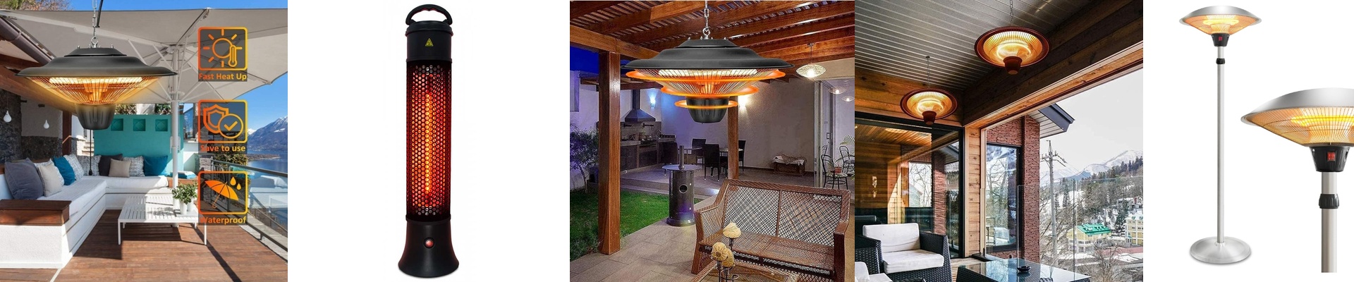
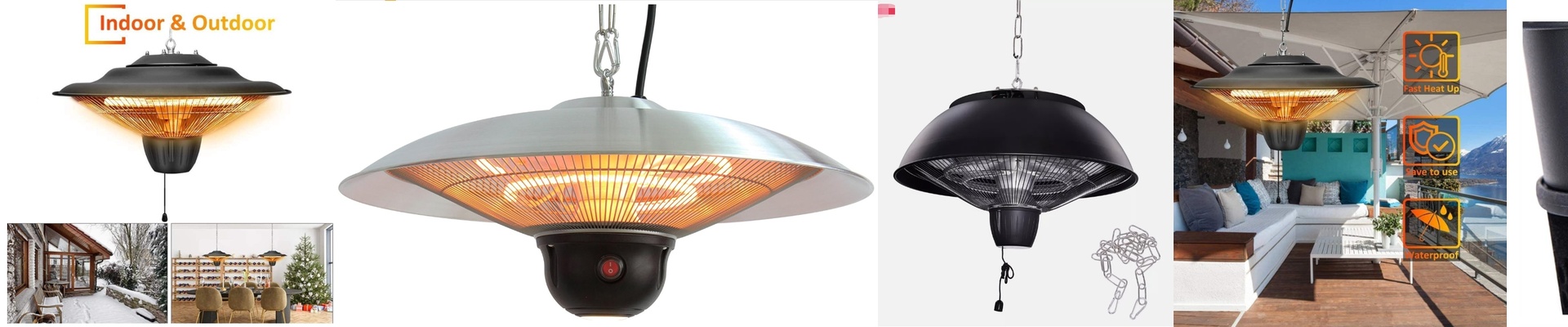

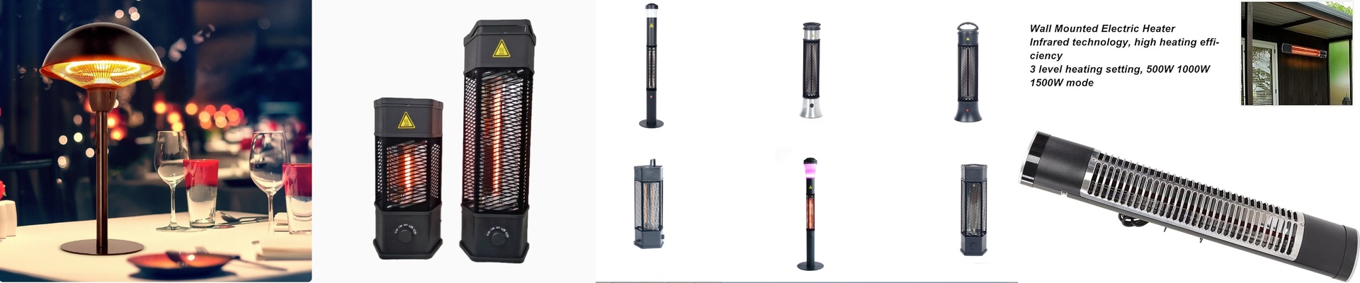
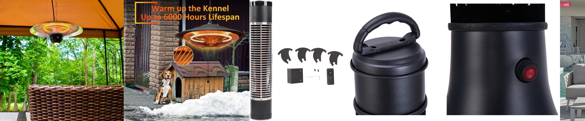
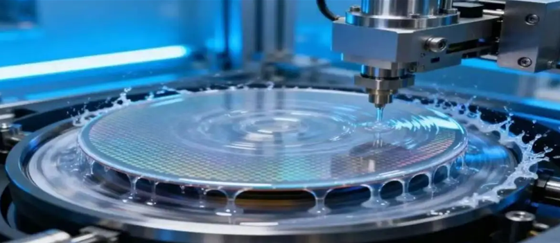
On the fab floor, a photoresist bake isn’t just another thermal step—it’s your thermal budget. Push even half a degree off target and you’ll see critical dimension drift and yield loss, lot after lot. That budget is enforced where the heat is shaped: the reflector in the wafer curing lamp. What matters, technically We build the reflector to match the spectrum of halogen and short-wave IR sources, so energy lands where it should—on the wafer—without dumping stray heat onto optics and stages. Surface finish and geometry are held tight so the bake zone hits wafer-level temperature uniformity within ±0.1°C. The substrate is ultra-pure quartz or high-grade ceramic, chosen specifically for low outgassing and zero particle shedding. In Class 1–100 cleanrooms, it keeps particle generation below spec, so the lithography environment stays clean. Why it holds up in production The reflector locks down both soft bake and hard bake profiles, so repeatability improves from lot to lot and edge bead variability drops. Tighter thermal control means you can trim bake time without hurting photoresist performance—energy use goes down and throughput goes up. The materials and coatings are built for 24/7 duty, delivering stable output over 5,000+ hours with minimal drift, which cuts unplanned downtime and reduces how often you swap lamps. Installation comes down to alignment: the reflector has to be dead-on with the lamp axis and the wafer plane. A misalignment of a few milliradians is enough to hurt uniformity and create hot spots. It drops into standard curing stations and can be specified to match particular lamp envelopes and mounting interfaces. If you’re running medium-wave or NIR sources, confirm spectral reflectivity and thermal load with the lamp maker—otherwise you risk cooking the reflector body. We design for the process, not the spec sheet. When the bake is controlled, it stops being a risk and starts being a repeatable variable you can bank on.